


Naprotek to Exhibit at International Microwave Symposium 2023
Join Naprotek in person at this year's International Microwave Symposium (IMS 2023) from June 11-16 in San Diego, California. We're excited to...
Transformation Capabilities with Accelerated Time-to-Test
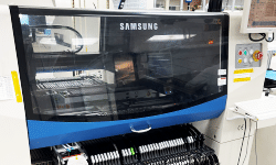
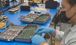
Built for Quality, Velocity, and High-Mix PCBA Manufacturing

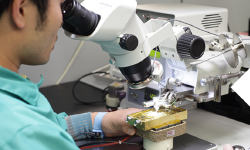
RF/Microwave Assembly and Testing to MIL-STD
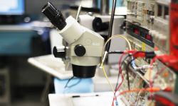
Fully Equipped RF Testing and Screening Lab to MIL-STD

Design for the Most Demanding Conditions in Harsh Environments
From Custom RF Circuits to Manufacturing Readiness

Delivering Quick Turn Printed Circuit Boards in about 1-5 Days
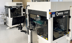
Producing Circuits with Speed with Rapid Change Management

Streamlining the Ramp-to-Production
Reduced cycle times for production

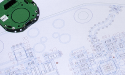
Complex and Dense ATE Boards
Turnkey Electrical and Quality Services Include MIL-PRF and MIL-STD Screening

Robust, Reliable and Repeatable
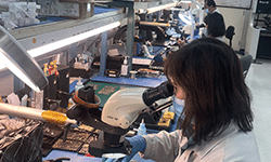
Collaborating Closely with Our Customers to Deliver Electronics Solutions

Sourcing from Distribution, Direct-from-Customer, or Kitting Partners
Flexible Sourcing with Turnkey, Consigned, and Hybrid Models

Leveraging the Precision of Ion Beam Milling vs. Chemical Etching of Thin Film Circuits
Next-Gen Anisotropic Ion Beam Milling Process is Proving to be Precise, Repeatable, and Clean

Our Business Development Team is
available to discuss your requirements.
